
One of the things I’ve made to understand how the Compustar works is to reverse engineer its schematics.
Now I’m publishing this schematic and a 3D rendering of the board both to explain in little more details how it works and to aid anyone who has to repair it. This will be a two part series, this time the microprocessor board, then, in a few months, the display board.
Update October 5th, 2017: Part 2 is here: https://www.aemfoto.it/wp/2017/10/05/the-compustar-schematic-part-2-the-display-board/
To avoid doing a single giant sheet, I divided the schematics into multiple pages. Let’s see the pages one at the time, with a little of description.
Since there is no silk screen on the board, the designators (IC1, R1, and so on…) are just made up, and may also be quite randomly assigned. Moreover, I’ve not put in the schematic all the 100nF bypass capacitors (while all the other capacitors should be documented). I’ve also left out a 220 Ohm resistor located near the buzzer/speaker, since I did not understood where is was connected.
Clock generation

This part of the Compustar generates all the clock signals used, except for the ones generated internally to the CPU.
Two similar circuits are used.
The first one uses a 7MHz oscillator done using a crystal with a few passive components and a couple of inverters. A third inverter (IC11B) buffers the output for the divider, a single 74HC4020 (IC3). Three different frequencies are generated: 3.5MHz (used by the 8254 timer chip), 27.34kHz (7MHz / 256, used as a clock for the CPU timer #0) and 13.67kHz (7MHz / 512, used for the microstepping PWM).
The second oscillator is similar to the first one, except for the crystal (which is a 4.9152MHz) and some component values. The generated frequencies are: 2.4576MHz (XTAL / 2, used by the 8254 timer for sound generation), 307.2kHz (XTAL / 16, used by the ADC). 153.6kHz (XTAL / 32, used as a clock for the CPU timer #1) and 38.4kHz (XTAL / 128, used as a clock for the CPU timer #2 as a baud rate generator).
Connectors
 There are 2 DB-9 connectors for the two joysticks, both similarly connected, with two analog inputs for the X and Y positions, two digital inputs for the two buttons, and a sense input to detect when a joystick has been connected. The only hardware difference between the two joysticks is the sense pin: on the side joystick (CN4) it is done using a digital input (P1.7), while on the center one (CN5) it’s done using an analog channel (AN5), probably because there were no more available digital inputs.
CN6 is the RS-232 port. Note that its pinout is not the standard one for a DB-9 connector, because the Compustar predates the use of 9 pin connectors as serial port connectors. So, a special cable is required to connect the Compustar to the RS232 serial port of a PC (or a USB/Serial adapter, nowadays). IC31 and IC32 are fairly standard level converters used to convert the RS232 signal levels (+12V / -12V nominally) to the TTL levels used by the Compustar.
CN1 is the connector to the Compustar Power Box. There are the power supplies (Ground, +12V for the serial port and voltage sensing, +5V for the logic board itself and a -5V – probably unused), the motor signals, and three spare/unused output pins I may use sometime in the future.
CN3 is the internal connector (via a 40 pin ribbon cable) to the display/keyboard board we’ll see in Part 2 of this post.
And finally, CN2 is an unused 26 pin internal connector . I don’t know which use this connector was for, but I think it may be either for some future expansion (never happened, unfortunately) or simply a factory test port.
CPU
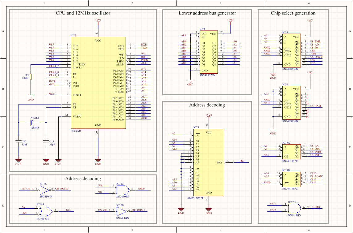 IC22 is the main 8052 CPU. It’s an old Intel microcontroller, with no internal program memory, 256 bytes (yes, bytes!) of internal RAM, three timers, one serial port and a few (8, here) I/O pins. This CPU, however, has two separated buses, both used here. One is for the program memory (64Kbytes, 32Kbytes used by the Compustar) and another is for the data memory (64Kbytes, in addition to the internal 256 bytes which are on a third internal bus). The two buses are multiplexed using just 16 pins plus a few other signals (RD/WR/PSEN/ALE). IC23 takes care of demultiplexing the Address lines from the Data lines.
If you think that multiplexing the bus slows down memory operations, you’re right. But this does not matter, since the 12MHz clock is divided internally and instructions takes from 12 to 48 cycles to complete. We’re in no hurry, here.
The remaining ICs in this page are used for address decoding and to generate the selection signals (chip selects, as they are called).
DEC Motor, RA Motor

 Both motors are driven in the same way. Using an output port (implemented by IC15 for the declination motor and IC14 for the RA motor) the microprocessor selects which signal is routed via IC7/IC8 (DEC) and IC5/IC6 (RA) to the motor windings. This signal can either be an ON, an OFF, the PWM generated by the 8254 timer (Timer #0 for the RA motor, and timer #1 for the DEC motor) or an inverted version of the same PWM. These signals are used to drive the windings both in microstepping and in full stepping with the exception of the PWM/Inverted PWM signal which is used when microstepping only, and not while moving using full/half stepping.
Memories
 On the two buses I’ve described in the CPU sheet, there are some EPROM programmed with the program itself and the object database.
IC24 is the 32KBytes main program EPROM, mapped on the Program memory bus. Even if the EPROM itself is 32KBytes, only 24KBytes are used for the actual firmware. The remaining 8Kbyes contains part of the object database. There is a jumper option (J1) to install a bigger (64KBytes) EPROM, but (Update 5th Oct 2017) a trace must be cut to do so.
IC25 and IC26 are two different EPROMs (IC25 is 32Kbytes while IC26 is just 16KBytes) containing the remaining 48KBytes of the object database.
IC27 is an unpopulated socket for an optional 8KBytes RAM chip, that was probably deemed not necessary later in the development cycle and therefore not installed. I’ve used this socket for the DS1643 Clock/Calendar/Non volatile RAM chip.
Miscellaneous
 A few different things in this sheet.
R10/R11 and C11 are the voltage divider to the ADC to read the +12V power supply, used by the original firmware to lighen “LOW BATT” when it was under a certain level, and that I’ve used, in my firmware, to display the actual supply voltage (DISP/SCOPE/REV)
IC1 is a voltage inverter used to generate a -5V from the +5V supply for the serial port drivers.
IC16C is the power on reset, which resets the Compustar at power up.
IC17E is the buzzer/speaker driver.
Peripherals
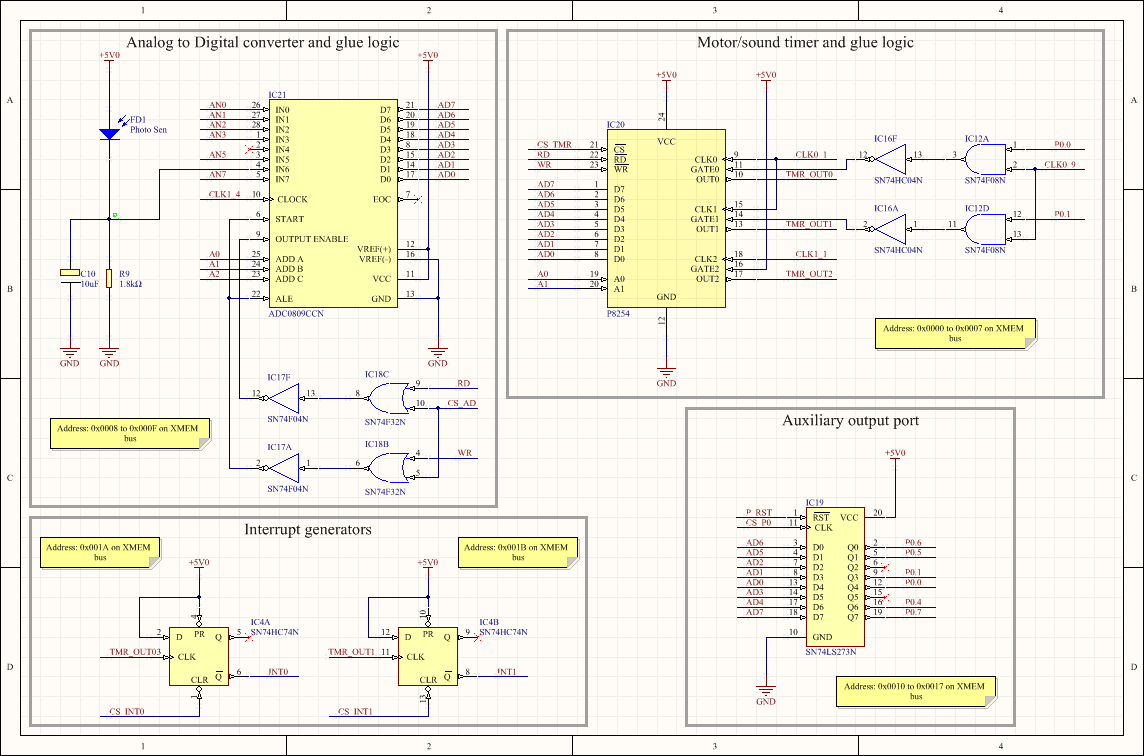 IC21 is an ADC0809, the Analog to Digital converter used to read the joystick analog inputs, the battery level and the “DAYLIGHT” photodiode. The firmware uses a round-robin schedule between the 8 channels to start the conversion and read the result back on each channel, using some “glue logic” ports.
IC20 is the 8254 timer chip. It has 3 timers. Timer #2 is used to generate the buzzer/speaker tones. It’s programmed with the desired tone pitch and started. It’s then stopped to end the note.
Timer #0 (RA) and TImer #1 (DEC) are used for the motors in two different ways. When the motor is stepping normally (during SLEWs, or when moving the telescope in SLEW speed) the timer generates the step timing the CPU uses (via IC4 and interrupts INT0, INT1) to change the motor phases. When, on the other hand, the motor is microstepping, the step timing is generated using internal CPU timer #0 (at a fixed frequency), while these timers are used to generate the PWM required for microstepping: the 13.67kHz clock from the clock generator circuit starts the PMW pulse (using the GATE pin) while the pulse length (and therefore the actual winding position) is controlled by programming the duty-cycle register in the timer itself.
IC19 is an auxiliary output port used to disable the GATE signal when not needed (P0.0 and P0.1), to drive a RS232 control signal (P0.4) and to drive some spare/unused signal wired on the Power box connector (P0.5, P0.6, P0.7).
The full PDF schematics/component layout
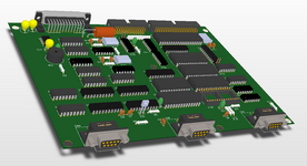 The full PDF schematics can be downloaded here, while this is the component layout.
I’ve also done a 3D rendering of the board in a 3D PDF, that can be downloaded from here (warning! big file, 13MBytes!)
Note: these PDFs (expecially the 3D rendering) will probably be rendered incorrectly by the internal PDF viewer of either Firefox or Chrome.
Update October 5th, 2017. Fixed an error in the schematic on IC24: Pin 1 is directly connected to VCC. I missed a small PCB trace.
4 commenti
Vai al modulo dei commenti
Brilliant! But what is the DAYLIGHT photodiode used for? Surely it does nothing when the box is closed?
Randy John
Autore
It’s read by the ADC and used to highlight the “DAY TIME” label (located above the “SMALL’R THAN” label on key 6). You can try this with the emulator (View/Flags/DayTime). I’ve never tested if this work on the real Compustar, though. As you noticed, the photodiode is inside the box, but it is near the opening for a DB-9 connector, so maybe some light filters in…
Ciao
Angelo
Angelo,
I powered up my Compustar 8 for the first time in years. I blew a cap in the display (C15). I replaced that and blew two more Tant’s in the power box. They are the two big ones next to the TO-3 and the fan. Any idea what the values are?
Randy John
Never mind. All three caps are 47uF/16v. I replaced two and it’s working now.
Randy